SEGA Flash Card V2 (and stand-alone mapper)
The original SEGA Flash Card, while working, needed a new revision made entirely with freely available software and free software where available. It would also be useful to separate the mapper into its own module as to allow using it on any other projects.
The main objective is making this second revision of the SEGA Flash Card freely available for anyone to use, modify and sell if so they wish, implying it would require using free and open source software where available. To this effect, the circuit boards have been designed in KiCAD instead of a barely-legal version of Labcenter’s Proteus, and being free from the license restrictions of Proteus, I can now release the boards under a free license like the Creative Commons BY-SA 4.0 and the firmware source code under the MIT License.
TL;DR: You can almost do whatever you want with this project as long as you give the author credit. Project source code available here.
January 2021: Someone needed them so now the schematics of the flash card and the SEGA mapper in PDF are now available for download.
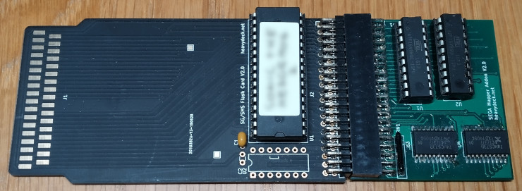
The Card PCB
The main card PCB required a major fix, namely changing its thickness from 1.6mm to 2mm, and removing all the mapper logic away from it. For this reason the main card PCB only contains an SST39SF040 ROM chip, a 40-pin header for an external mapper or hardware, and an optional place where a 74HC32 IC could be installed if the board is to be used as a plain 32K card.
The board width has been reduced a small bit as to prevent scratching of the console card slot, and finally, as an additional precaution, no vias where placed too deep inside the console since it contains a ground shield that might make contact with the card top.
All in all, the resulting physical dimensions are as follows:
Mapper module
The mapper module follows the same design as the previous revision with all the logic on the same board and a 40-pin header connector as to be attached to the flash card. The main difference is the usage of a single 74HC573 8-bit latch for each mapper bank (instead of two 4-bit latches per bank) and the usage of SMD components instead of Through-hole ones. Otherwise, the design is exactly the same with a 16V8 GAL to do the address decoding and another 16V8 GAL implementing the logic.
Notice the pin connector has three rows. This is intentional as to allow using both 90º pin sockets (which would use the bottom two rows) or use a far cheaper straight pin socket (using the top two rows) because by design, the top row and the bottom row are the same, allowing this “rotation” of the pin socket.
Finished result
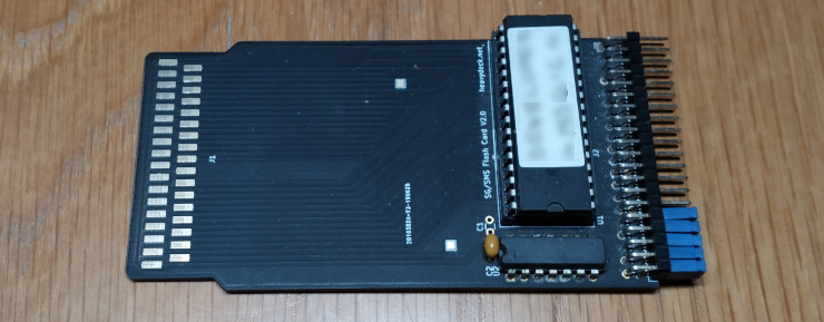
These are flash cards on its two configurations. The basic 48K configuration with no mapper, mainly used for loading homebrew and testing programs:
And the fully assembled cartridge with mapper, able to run commercial games that use SLOT1/2 mapping.
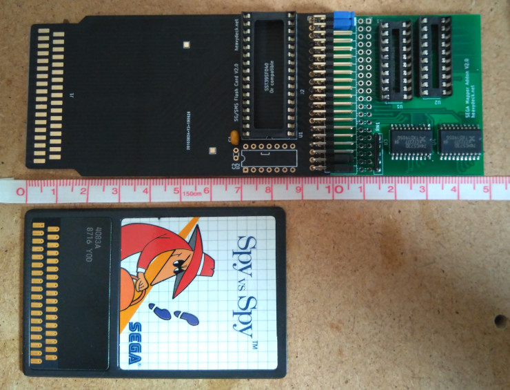
For comparison, here’s a partially assembled cart against an original “Spy vs Spy” SEGA card game.