SEGA Master System flash card

Update: A newer revision is available with PCB design documents, firmware source and binaries.
This project attempts to make a programmable SEGA Master System card which would allow loading custom programs or existing games on the Master System console through its card slot. The motivation behind this project has been being able to quickly develop software for the console, especially cartridge dumping tools since the Card Slot boots first on unmodified systems, and of course being able to play old SEGA games the way they were intended. On the console itself.
The SEGA Master System (SMS from now on) is an 8-bit console, contemporary to the Nintendo NES and other 8-bit consoles of the time. I’ve had this console around since… forever, and I played the few games I had more times than I can remember. Some time ago I wanted to play some of the games I never had so I did what anyone would do. Download an emulator, some ROMs and get playing. However, having the machine itself it felt like a waste not to try to run the ROM dumps on the hardware itself.
This idea led me to study how the console works, a failed prototype, and finally being able to play Ecco the dolphin on the console 20+ years after its release.
Design
The SMS is an 8-bit console built around the Zilog z80 CPU, this CPU has an 8-bit data bus and a 16-bit address bus, which are shared among the different peripherals, ROM chips and RAM chips. The system memory map has 48K available for ROM and 16K reserved for RAM. To allow using larger ROMs SMS cartridges usually have a mapper chip on the cartridge itself, be it a discrete chip or built into the game IC.
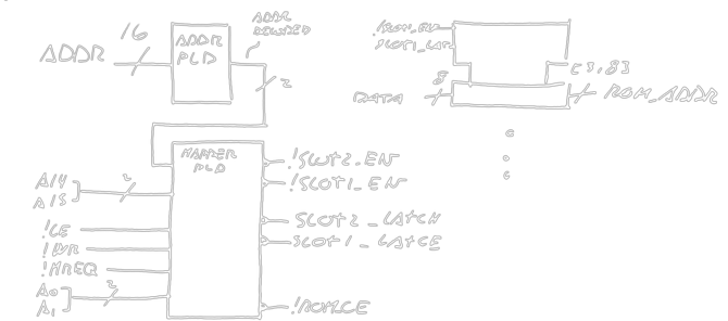
Design phase drawings done in PaperCAD :P
Minimal cartridge
The bare minimum cartridge design would provide 32K of ROM space and needs minimal components. Any ROM chip and an OR gate (74LS32 or similar) is enough.
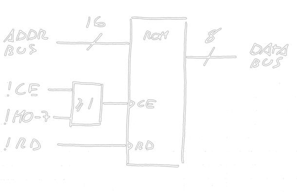
!M0-7 signals with a low level whether the address bus is within the [0x0000 0x7FFF] range, is equivalent to the A15 line in places where either of them is not available. The Address bus, Data bus and the !RD signal are connected. This design will allow up to 32K as stated above.
The SEGA mapper
To push past the 32K barrier, different mapper chips will change the upper address bits of a larger ROM depending on the current z80 address range. Conceptually the mapper sits between the CPU buses and a ROM’s upper address bits. The SEGA mapper selects these bits depending on the current address, dividing the address space in four 16K slots. To set these upper bits for each slot, the mapper chip will accept write operations at predetermined addresses.
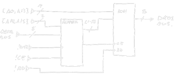
The SEGA mapper design allows up to 4MB ROMs to work although ROMs above 512KB are uncommon.
Replacing the SEGA mapper
To make a replacement of the SEGA mapper I’ve decided to use the absolute simplest components I could find, using discrete components of the 74xx series where useful so, for every SLOT I will be using a D-Latch with 3-state outputs as a register, outputs connected to the ROM’s Address bits starting at A14. A circuit will select either slot register and write the value on each register where required.
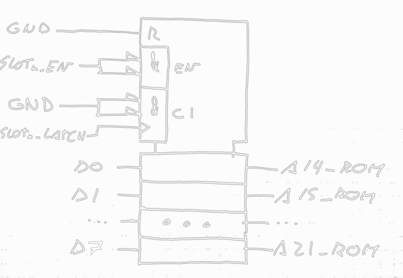
To select each slot we will activate each register depending on the value of
[A14, A15], Selecting SLOT2 on 10 SLOT1 on 01 and SLOT0 on 00. Current
design only implements SLOT1 and SLOT2. To Latch-in a value into a register it
needs to detect memory writes to addresses on the [0xFFFC 0xFFFF] range. I’ve
decided using currently available 16V8 PLDs since they are 5V compatible,
cheap, and I had the programmer readily available. The card design uses Two 16V8
PLDs, one to decode the Address value and the other to control all the slot
enabling, latching and ROM enable.
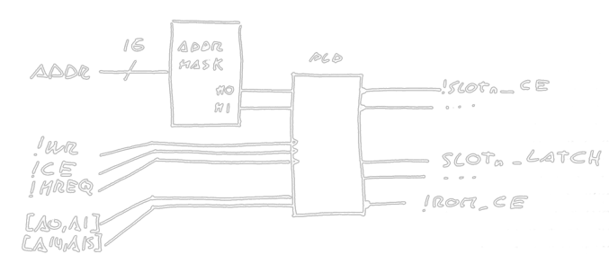
A high level overview of the whole thing:
Making it real
Lacking any precise measurement of an original SEGA card, the reasonable thing was getting one. Five minutes on eBay did the trick, with the added bonus the seller sent me the wrong card so, even though I did not intend to play that game, I got a nice discount just in case. At SMS Power there is the pinout of the card, showing we have every needed signal and bus to do our job.
After measuring my unintended copy of Spy vs Spy decided to make the cartridge a two-board solution where the known and tested connections (things like data bus, the lower range of the address bus and some signals) would be wired on the board entering the console, and any connections and buses useful for creating a mapper would be connected to a series of pin sockets where a daughter board could be connected. Main reason behind this decision was being able to fix potential hardware errors more easily if they ever happened.
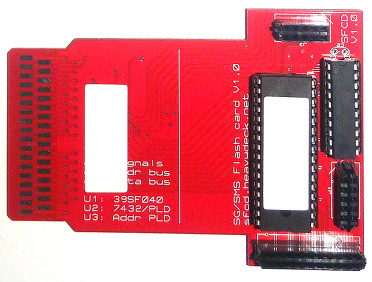
So the main board would contain the ROM chip (512KB SST39SF040 flash), the address decoder PLD (An ATF16V8B) and the mapper PLD (another ATF16V8B). The data bus is exposed to pin headers while only the address decoder lines, A0, A1, A14 and A15 of the data bus would be exposed to header pins. Additional signals like the mapper PLD outputs and the ROM upper address pins are also exposed to the header pins.
The base board schematic ends up being:
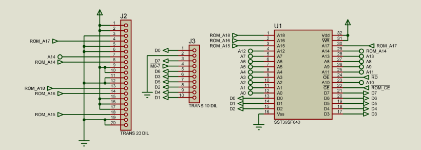
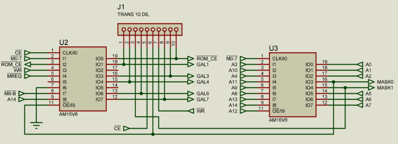
The PLD socketed on U2 has been wired in such a way that a 74LS32 circuit can be placed there instead of an ATF16V8 to make a 32K ROM card.
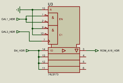
To implement a functional mapper for most SMS games I would need at least SLOT1 and SLOT2 mapping, and to address a 512KB ROM in 16K slot, it would need to provide one 5-bit register for each SLOT. Due to availability issues I opted to use twin 74LS173 4-bit D-latches with 3state outputs (HC family circuits can also be used here). The output of the register is pulled down on ROM A15 to A18, ROM A14, if left floating (during SLOT0 reads) will get whatever level the z80 A14 line has. For each SLOT register, the inputs will be connected to the z80 data lines, and outputs to the ROM upper address lines. It will also require two connections to the Mapper PLD for each SLOT register, one for enabling the register output and another one to latch-in a new value into the register.
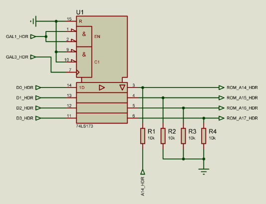
Notice the second D latch is slightly underused but is still necessary for the fifth bit.
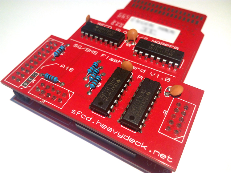
The final result
The finished boards, fully assembled.
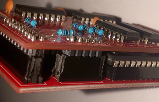
It is working!
Below are some pictures of the cartridge working on the console, with “Chuck Rock 2” (a SLOT2-only game) and “Ecco the dolphin” (A SLOT1/2 game). Pardon the lab’s appearance :P


