Micro85: An i8085 microcomputer

Having found some i8085 CPUs not so recently I decided to make a proper microcomputer with them, providing it with common peripherals like RS-232 ports, and some not so common for the day peripherals like an LCD screen and a DMA controller. On this page I will be documenting the projects as it gets developed.
KiCAD project and PLD source code available on source repository.
i8085 Basics
The i8085 is an 8bit CPU requiring a single supply 5V supply voltage, making it a popular choice for microcomputers and control systems on early 80s. It has a 16bit Address bus, giving up to 64K of directly addressable memory, and an 8bit IO address bus, giving up to 256 IO devices. The address bus is multiplexed with the data bus as to save pins on the DIP40 package, allowing for more interrupt options (5 interrupt lines) compared to other contemporary CPUs like the Z80 or the 6502 which usually have two but have un-multiplexed address bus.
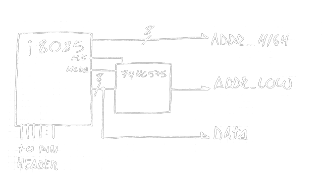
At its most basic, the i8085 requires some memory and an 8bit latch to
demultiplex the address bus. The standard 74HC575 (or any CMOS variant of the
74 series) works fine to do this job. Connecting the !OE and load signals
to the relevant i8085 pins.
For the Micro85 memory layout I’ve decided to give it 64K of memory, either a
32/32 split of ROM/RAM or using the full 64K for RAM and having a way to
bootstrap the program to RAM before bringing up the i8085 CPU from reset.
The address decoder takes the IO/!M and the A15 address bit and with some
glue logic (using a single 74HC00) select the correct 32K memory chip !CE
line.
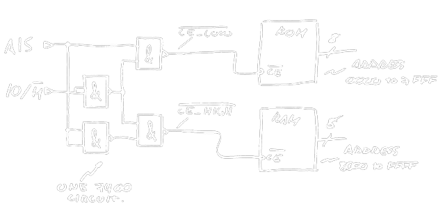
Update: While the memory layout remains the same, the 74HC00 decoding has
been moved into a dedicated address decoder implemented with an ATF16V8 PLD.
GPIOs
Having some uncommitted IO pins is always useful. Implementing some GPIO is
as easy as having some addressable latches where the CPU can latch in some
values for output and assert the data bus to read some inputs. Having extra
available 74HC575 from the CPU address made them the obvious choice.
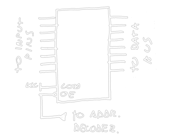
Inputs are a transparent latch with load always asserted and the !OE
signal connected to an address decoder, so when the CPU reads the correct
IO address, the !OE line gets asserted and the inputs become available to
the Data bus.
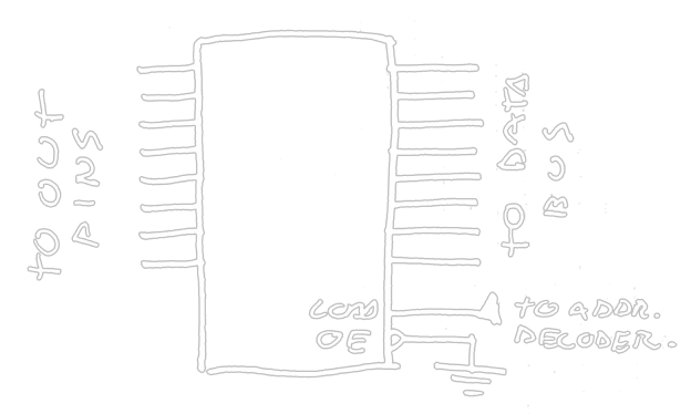
Conversely, outputs are a transparent latch with the !OE always asserted
and the load signal connected to the address decoder so when the CPU writes
to the appropriate address, the value on the Data bus gets latched into the
output pins.
Since inputs are CMOS it would be a good idea to pull them to any value or connect them to the nearest output if not used.
Serial ports, storage and DMA
For the remaining peripherals, namely two serial ports and some form of bulk storage, the easiest way to do it with reasonably priced hardware would be using a microcontroller to manage these “high speed” peripherals and use DMA and interrupts to move data to/from the CPU and peripherals.
DMA
Direct Memory Access DMA is essentially a way for peripherals to access the system main memory without involvement from the CPU. This frees the CPU from the work of moving the data to/from peripherals, increasing the efficiency of the system overall. A typical DMA transaction goes something like this:
- CPU requests the peripheral to do some work
- CPU continues to do other work
- Peripheral does its work and writes result to main memory
- Peripheral triggers a CPU interrupt, signaling work is completed
On the i8085 the CPU has control over the buses during normal operation, so
peripherals should not be able to take control of the main memory to read or
write data from it. To make the CPU “give up” control of the buses, the i8085
provides the HOLD and HLDA pins. Asserting HOLD will tell the CPU to
relinquish control of the buses as soon as possible. Once asserted, the data
bus, the address buss and the !RD !WR IO/!M pins will go to high
impedance mode, allowing for other circuit to assert those lines. Once the
buses are free to be used, the i8085 asserts the HLDApin signaling other
circuits that the bus is indeed free to be used by others.
So, on our i8085, a peripheral-to-memory access is like this:
- Peripheral finishes task
- Peripheral asserts
HOLDsignal and waits forHLDA - CPU gives up control of buses, asserts
HLDAand pauses execution - Peripheral writes data to main memory
- Peripheral deasserts
HOLDsignal - CPU regains control of buses and continues execution
- Peripheral triggers a CPU interrupt (
RSTxTRAPorINTpin)
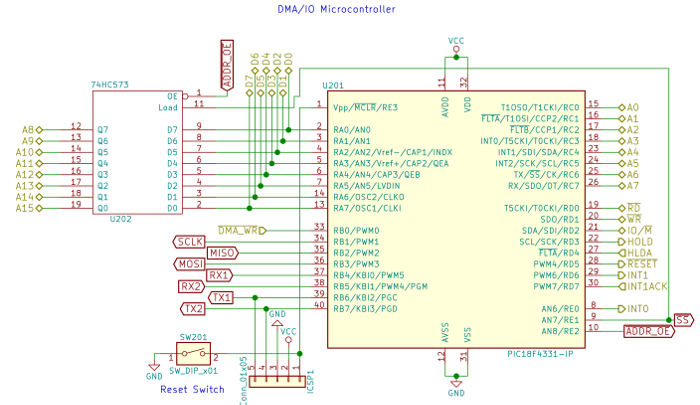
The DMA controller
Out of convenience and familiarity I’ve chosen a PIC18 (which probably has more computing power than the i8085) to do all the IO/Memory workload. It also comes with many useful peripherals out of the box like two UART ports and two SPI/i2c peripherals as well. This gives me an obvious solution as to how to give the i8085 access to both serial ports and storage (SD card or Flash via SPI/i2c) without having too many or too obsolete circuits.
A PIC18 microcontroller on a DIP40 package will have 36 GPIOs for you to use.
Doing the math this circuit will have to control 16 bits for the address bus,
8 bits for the data bus, the IO/!M !RD !WR HOLD HLDA signals, 4 more
pins for the two serial ports, 3 interrupt lines RST5 INT INTA, one
incoming (CPU-to-DMA) interrupt line, 4 pins for an SPI peripheral (SD card)
and a couple more lines I find interesting like !RESET or the PIC18 (!MCLR)
own reset line.
Add all up and it gives… 43 pins. D’oh!
Checking the i8085 you can notice the trick it uses to get some more IO pins
while keeping the DIP40 package by multiplexing the data/address lines, so I
decided to do the same in order to “save” 6 pins (-8 address bits + latch
!OE and load) putting me on the 37 pin count, almost fitting on the pin
budget I have. Multiplexing two other signals would put me just enough to fit
all the IO I wanted on this circuit, so I decided to mux the address latch
load signal with the SPI !SS signal since at no time would those two be
used at the same time. Spurious load asserts don’t matter and spurious
!SS asserts wont matter as long as the clock is kept quiet.
As a minor side note, unlike the i8085 the lines I will be multiplexing are the data bus (direct) and the upper address byte (latched) since changes to the upper address byte on bulk, sequential memory transfers are less common than changes on the lower address byte, giving the PIC18 some room for performance improvements.
Serial
The chosen PIC18 has two UART ports, which will be DMA-accessible. One of the
ports will be connected to a MCP2221A USB-to-Serial bridge. This port will
also double as the power source for the whole board. The second UART port will
be connected to a MAX232 UART-to-RS232 bridge so regular serial port
peripherals can be connected to it, like an old-fashioned dial-up modem. I may
consider adding the option to disable either of those bridges in order to, if
needed, have a 0 to 5 Volt serial port.
Storage
The same PIC18 also has two SPI/i2c controllers, the relevant CLK MOSI
MISO and !SS lines will be exposed on a 6-pin header together with Vcc
and GND so an external SPI flash or an SD card can be added to provide
storage to the board. Just like the serial ports, it will be DMA-accessible
to the i8085 CPU.
Circuit design
Time to get busy and make the microcomputer real. This is my first proper project where I will be using from start to finish as much free (as in freedom) software as I can. That means ditching some less than legal CAD programs and actually learn to use KiCAD for once.
KiCAD is a pretty powerful suite but the learning curve is a bit more steep than
Labtec ARES/ISIS or Altium since the most likely answer for “Does it have this
component?” is “No” so you will need to know early in the process how to make
new components or half-ass your way and find a pin-compatible component.
Common hacks are using whatever PIC18 you can find since they are mostly pin
compatible, same goes for HC AC HCT variants of the old LS circuit
series.
A brief description of some of the microcomputer building blocks will follow.
CPU interface
Like on the design above, the i8085 has a latch attached to it to store the
lower address byte and the memory address decoder has been implemented on
an ATF16V8 PLD where the IO/!M signal active value is dependant on
whether the address line A15 is active or not. Additionally, all signals that
need it have been pulled up or down to their inactive state, with the exception
of READY and RESET which are pulled to their active state, meaning the
board will start with the CPU held on reset and the memory will be accessed
as fast as the CPU will try.

IO/DMA controller
In a similar manner, the IO/DMA controller will be using the same ‘hack’ the
i8085 uses to save pins by multiplexing one byte of the address bus only on
this case the high byte is latched. Aside from the memory interface, the
peripherals are directly attached to available pins on the PIC18, and the
SPI !SS pin is multiplexed with address latch load signal.
A programming header has been placed in such a way that it should be usable
with the whole system online, at most losing some of the serial port
functionality. Additionally, a physical reset switch has been added to the
PIC18 !MCLR pin in order to reset both the PIC18 and the i8085.
Note: Golden pins are connections to the i8085 CPU or the Address decoder.
Making a Prototype
Boards have been ordered and the process of making this a reality starts now.
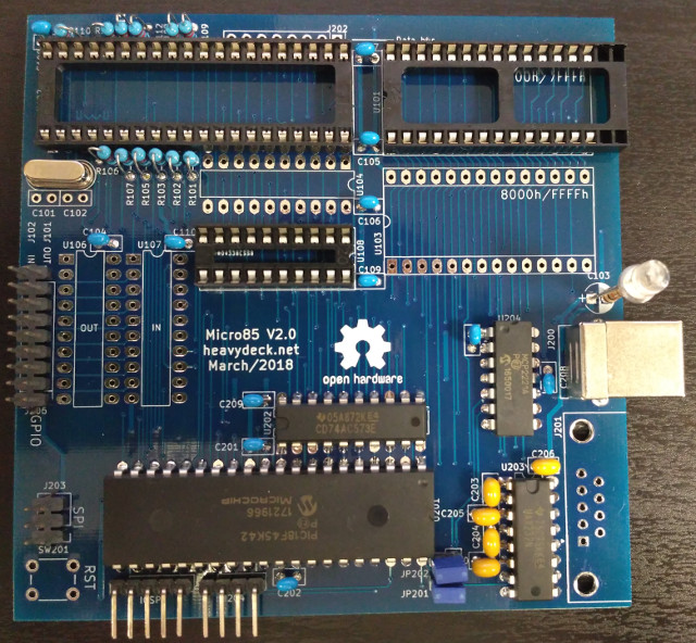
2018, April 10Th: Boards just arrived and I had to partially assemble at least one of them to test the serial interfaces and the address decoder with the PIC micro. Here’s a pretty pic of it.
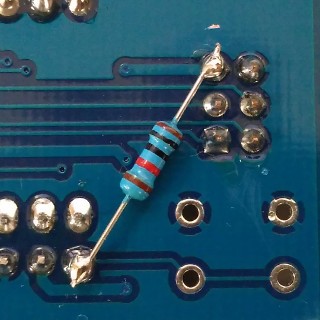
The USB interface seems to be working correctly as is the ICSP programming header. On the (literal) flip side, the internal pull-up of the MCU reset line is way too weak, to the point that putting a finger near that track can reset the MCU. As a result, I had to quickly add an unplanned pull-up.
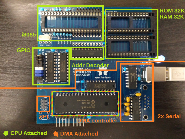
Just for show, these are the building blocks of the microcomputer showing if a peripheral is directly attached to the CPU bus (i8085 can access it without DMA) or if a peripheral is strictly DMA attached.
First DMA writes/reads
2018, April 17Th: Been developing the IODMA firmware. As of now it can make some Power up self tests (like detecting RAM/ROM and DMA address, and at last some writes to RAM were made via DMA.
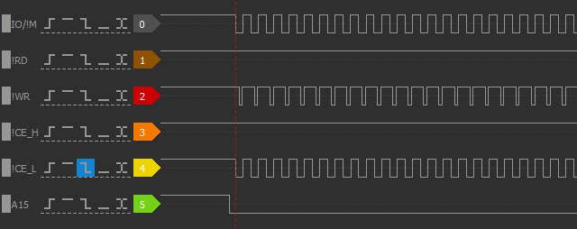
Here a DMA write to low RAM is seen using a logic analyzer. Pretty~~
More to Come!
This project is ongoing! Will update as development continues :)